
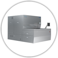
Phoenix HDI
 AOI for HDI and multi-layer PCB with min line/space down to 30 µm.
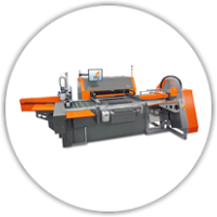
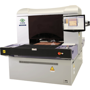
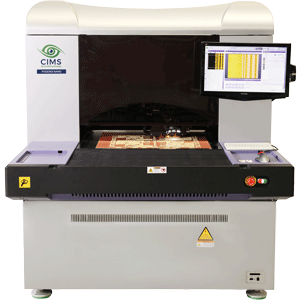
Phoenix HDI, CIMS latest generation of AOI system, is designed to support high volume manufacturing of HDI and multi-layer PCB. It is capable to scan down to 30 µm line/space width technology.
The system’s state of the art optical technology Microlight™ provides optimal light coverage in order to be able to meet the most rigorous detection requirements. Optimized performance is achieved by combining superior image quality with customizable detection algorithms.
Equipped with the state-of-the-art image acquisition and advanced software capabilities, the Phoenix HDI product family is renown for its exceptional detection achieved with lowest possible false calls rate.
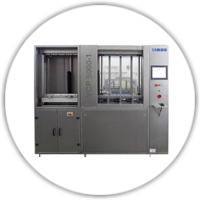
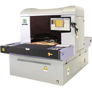 Phoenix HDI is powered by Spark™ 2.0 - an innovative cross-platform detection engine.
Basic functionalities include
- Multi-Step and Multi-Zone for best detection policy set-up per zone
- Micro Inspection and metrology engine
- Fully automated set-up
- Variable continuous resolution defined automatically
- Cad Analyzer creates best reference for detection
- Dynamic Job enabling operators to instantly change:
• resolution, steps, parameters on the AOI - Filtering system – Inspection results can be re-processed on AOI / CVR and present defects immediately after filtering
- Full automatic (BLACK BOX) Data Processing and Preparation from CAM Station
System highlights
- New linear motors for smooth & silent motion
- Robust structure
- Automated vacuum table
- Microlight illumination
- 64 bit based firmware
- Powerful processors to handle high density PCB
- Compatible with front or back L/U automation
- Simple and quick setting for new jobs
Optional Features
- +2DM metrology - panel dimensions measurement
- +2CD metrology - 2D measurments of circuit elements
- FI - final inspection for finished bare boards
- LDI - laser drill inspection
- CDB/CDBIC - defects classification and virtual defects mapping
- VVS - virtual verification system

All information subject to change without notice!
 Equipped with the state-of-the-art image acquisition and advanced software capabilities, the Phoenix product family is renown for its exceptional detection achieved with lowest possible false calls rate.
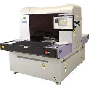
 Phoenix Nano is powered by Spark™ – an innovative cross-platform detection engine
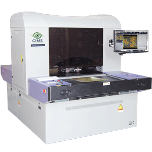 Basic functionalities include
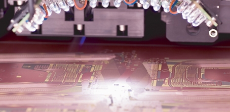 Optional Features